How was the image taken? Did you use any sampling or preparation methods that you think are interesting?
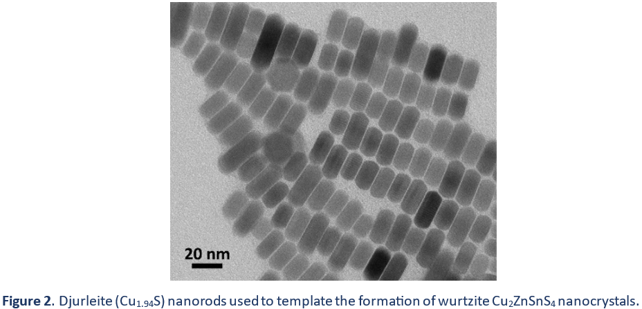
FYV: I acquired this image using a transmission electron microscope (TEM) operating at 100 kV. I thank Ilya Gourevich who trained me on how to operate this microscope.
The as-synthesized kesterite nanocrystals are covered by oleylamine molecules (long fatty amines). These long-chain surface molecules allow nanocrystals to be dispersed in non-polar solvents such as hexanes or toluene, making them easily processable into inks. However, these long molecules can be problematic in electron microscopy because they burn under the electron beam and create a blurry image. Therefore, these molecules need to be minimized for TEM measurements.
To remove a portion of these molecules from the nanocrystal surface, I had to perform multiple purification cycles using an anti-solvent (a bad solvent). This precipitates nanocrystals and removes some ligands from their surface. Then, samples can be dispersed back into solution with a good solvent like hexanes. The challenge here is to find a sweet spot where you remove enough ligands to prevent burning under the electron beam, but not so many that your samples remain aggregated and cannot be brought back into solution for subsequent drop casting. Finally, the samples are drop cast onto a carbon support on a copper grid and dried under air for imaging.
The purified nanocrystals in this sample randomly assembled on the grid and generated the South American-looking pattern seen in the TEM image, which coincidentally is where I am from (Chile).
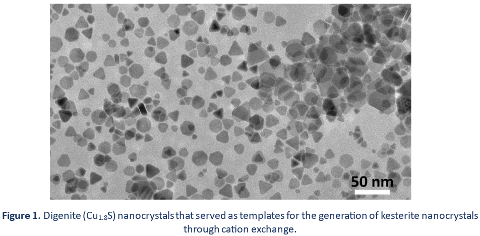
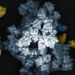
SG: The image was obtained through Transmission Electron Microscopy (TEM), using a copper mesh grid to support the crystals with a working voltage of 80 kV.
FLG: The image was taken using a Scanning Electron Microscope (SEM). For the preparation I spread a thin layer of zeolite powder onto a stainless-steel stub with carbon tape and then the sample was sputter coated with a thin gold layer.